Product
Plexda SFP+, SFP, SFF, QSFP, CFP, Ethernet media converter, POE switch,200G AOC cable OEM factory
Plexda SFP+, SFP, SFF, QSFP, CFP, Ethernet media converter, POE switch,200G AOC cable OEM factory

Tel:0755-28482291
Hotline:13728624948
Local:Home > Product > Optical Transceiver > SFP module
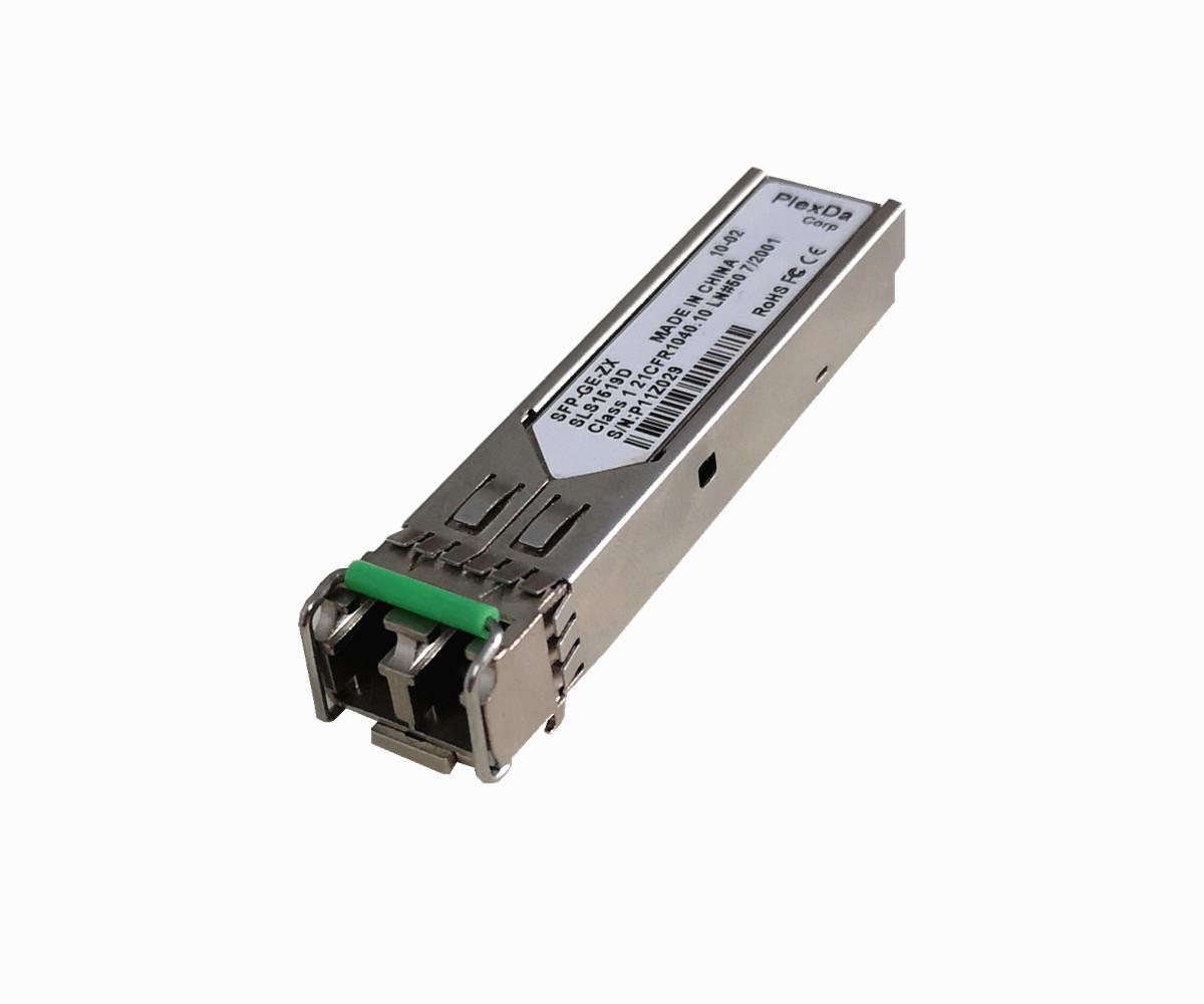
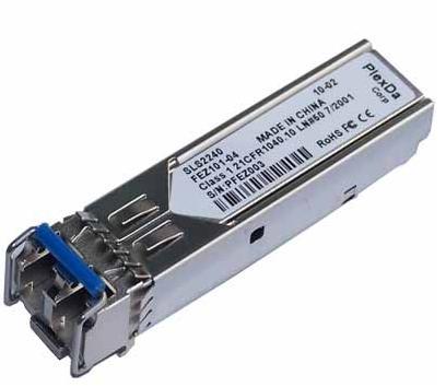
SFP-GE-ZX
1.25Gb/s Long-Wavelength SFP Transceiver
Data Sheet
APPLICATIONS
1.25Gb/s 1000Base-EZX Ethernet Links
1x and 2x Fiber Channel
SONET OC-48 LR-2/ SDH STM L-16.2
Switch to Switch interface
Distributed multi-processing
Channel extender, Data storage
SONET OC-24, STM-1/ STM-4
PRODUCT FEATURES
Compliant with specifications for SFP MSA standard
Compliant with specifications for IEEE-802.3z Gigabit Ethernet Standard
Compliant with specifications for SDH/SONET/ATM standard Duplex LC Connector Built-in digital diagnostic functions for option
Uncooled 1550nm DFB laser transmitter, APD Receiver
Differential LVPECL inputs and outputs
Compliant with ANSI specifications for Fiber Channel applications at 1x or 2x FC
TTL signal detect indicator
Up to 2.5Gb/s bi-directional data links
Single Power Supply 3.3V
Hot-Pluggable SFP footprint Up to 100km on 9/125μm SMF at 1.25Gb/s, 80km at 2.5Gb/s Metal enclosure for lower EMI Extended operation temperature range: 0℃ to +70℃
SFP-GE-ZX SFP transceiver is a high performance and cost effective and short distances transceiver for serial optical data communication applications, The interface converters meet the SFP Multi-Source Agreement (MSA) specifications, This module is designed for Single-mode fiber operation at the wavelength of 1550nm, The transmitter section incorporates an advance DFB laser, with temperature compensation and automatic power control circuit (APC). The receiver is APD receiver.
The transceiver is a duplex LC connector transceiver, designed for use in 1x FC and Gigabit Ethernet and to provide a IEEE-802.3z compliant link at 1.25Gbps applications. The transceiver are hot-pluggable, the characterization is performed in accordance with Bellcore specification TA-NWT-000983. All of them are housed in a stainless package and the combination produces a component of high reliability.
Absolute Maximum Ratings

Operation Environment

Electrical Characteristics

Transmitter Optical Characteristics:
(Ambient Operating Temperature Ta=0°C to +70°C, Vcc = 3.0V to 3.6V)

Receiver Optical Characteristics:
(Ambient Operating Temperature Ta=-0°C to +70°C, Vcc = 3.0V to 3.6V)

Timing Characteristics

Block Diagram of Transceiver

Digital Diagnostic Functions
SFP-GE-ZX SFP transceiver support the 2-wire serial communication protocol as defined in ther SFP MSA. It is very closely related to the EEPROM defined in the GBIC standard, with the same electrical specifications.
The standard SFP serial ID provides access to identification information that describes the transceiver’s capabilities, standard interfaces, manufacturer, and other information.
Additionally, The SFP transceivers provide a unique enhanced digital diagnostic monitoring interface, which allows real-time access to device operating parameters such as transceiver temperature, laser bias current, transmitted optical power, received optical power and transceiver supply voltage. It also defines a sophisticated system of alarm and warning flags, which alerts end-users when particular operating parameters are outside of a factory set normal range.
The SFP MSA defines a 256-byte memory map in EEPROM that is accessible over a 2-wire serial interface at the 8 bit address 1010000X (A0h). the digital diagnostic monitoring interface makes use of the 8 bit address 1010001X (A2h), so the originally defined serial ID memory map remains unchanged. The interface is identical to, and is thus fully back ward compatible with both the GBIC specification and the FP Multi-source Agreement.
The operating and diagnostics information is monitored and reported by a digital diagnostics transceiver controller (DDTC) inside the transceiver, which is accessed through a 2 –wire serial interface. When the serial protocol is activated, the serial clock signal (SCL, Mod Def 1) is generated by the host. The positive edge clocks data into the SFP transceiver into those segments of the EEPROM that are not write-protected. The negative edge clocks data from the SFP transceiver. The serial data signal (SDA, Mod Def2) is bi-directional for serial data transfer. The host uses DA in conjunction with SCL to mark the start and end of serial protocol activation. The memories are organized as a series of 8-bit data words that can be addressed individually or sequentially.
For more information, please see the SFP MSA documentation.
Digital Diagnostic Specifications
SFP-GE-ZX transceiver can be used in host systems that require either internally or externally calibrated digital diagnostics.

PINOUT TABLE

General Specifications

GBIC Serial ID Memory Contents

Serail ID Memory Contents: (A2h)
Address | #Bytes | Name | Description |
00-01 | 2 | Temp High Alarm | MSB at low address |
02-03 | 2 | Temp Low Alarm | MSB at low address |
04-05 | 2 | Temp High Warning | MSB at low address |
06-07 | 2 | Temp Low Warning | MSB at low address |
08-09 | 2 | Voltage High Alarm | MSB at low address |
10-11 | 2 | Voltage Low Alarm | MSB at low address |
12-13 | 2 | Voltage High Warning | MSB at low address |
14-15 | 2 | Voltage Low Warning | MSB at low address |
16-17 | 2 | Bias High Alarm | MSB at low address |
18-19 | 2 | Bias Low Alarm | MSB at low address |
20-21 | 2 | Bias High Warning | MSB at low address |
22-23 | 2 | Bias Low Warning | MSB at low address |
24-25 | 2 | TX Power High Alarm | MSB at low address |
26-27 | 2 | TX Power Low Alarm | MSB at low address |
28-29 | 2 | TX Power High Warning | MSB at low address |
30-31 | 2 | TX Power Low Warning | MSB at low address |
32-33 | 2 | RX Power High Alarm | MSB at low address |
34-35 | 2 | RX Power Low Alarm | MSB at low address |
36-37 | 2 | RX Power High Warning | MSB at low address |
38-39 | 2 | RX Power Low Warning | MSB at low address |
40-55 | 16 | Reserved | Reserved for future monitored quantities |
56-59 | 4 | RX_PWR(4) | Single precision floating point calibration data-RX optical power Bit 7 of byte 56 is MSB. Bit o of byte 59 is LSB |
60-63 | 4 | RX_PWR(3) | Single precision floating point calibration data-RX optical power Bit 7 of byte 60 is MSB. Bit o of byte 63 is LSB |
64-67 | 4 | RX_PWR(2) | Single precision floating point calibration data-RX optical power Bit 7 of byte 64 is MSB. Bit o of byte 67is LSB |
68-71 | 4 | RX_PWR(1) | Single precision floating point calibration data-RX optical power Bit 7 of byte 68 is MSB. Bit o of byte 71 is LSB |
72-75 | RX_PWR(0) | Single precision floating point calibration data-RX optical power Bit 7 of byte 72 is MSB. Bit o of byte 75 is LSB | |
76-77 | 2 | TX_I (Slope) | Fixed precision floating point calibration data – RX optical power. Bit 7 of byte 76 is MSB, bit o of byte 77 is LSB. |
78-79 | 2 | TX_I (Offest) | Fixed decimal(signed two complement) calibration data, bit 7 of byte 78 is MSB, bit 0 of byte 79 is LSB. |
80-81 | 2 | TX_PWR(Slope) | Fixed decimal (unsigned) calibration data, transmitter coupled output power. Bit 7 of byte 80 is MSB, bit 0 of byte 81 is LSB. |
82-83 | 2 | TX_PWR (Offset) | Fixed decimal (signed two complement) calibration data, transmitter coupled output power. bit 7 of byte82 is MSB, bit 0 of byte 83 is LSB. |
84-85 | 2 | T (Slope) | Fixed decimal (unsigned) calibration data, internal module temperature. Bit 7 of byte 84 is MSB, bit 0 of byte 85 is LSB. |
86-87 | 2 | T (Offset) | Fixed decimal (signed two complement) calibration data, internal module temperature. bit 7 of byte86 is MSB, bit 0 of byte 87 is LSB. |
88-89 | 2 | V (Slope) | Fixed decimal (unsigned) calibration data, internal module supply voltage. Bit 7 of byte 88 is MSB, bit 0 of byte 89 is LSB. |
90-91 | 2 | V (Offset) | Fixed decimal (signed two complement) calibration data, internal module supply voltage. bit 7 of byte90 is MSB, bit 0 of byte 91 is LSB. |
92-95 | 4 | Reserved | Reserved |
96 | All | Temperature MSB | Internally measured module temperature |
97 | All | Temperature LSB | |
98 | All | Vcc MSB | Internally measured supply voltage in transceiver |
99 | All | Vcc LSB | |
100 | All | TX_ Bias MSB | Internally measured TX Bias current |
101 | All | TX_ Bias LSB | |
102 | All | TX Power MSB | Measured TX output optical Power |
103 | All | TX Power LSB | |
104 | All | RX Power MSB | Measured RX input optical power |
105 | All | RX Power LSB | |
106 | All | Reserved MSB | Reserved for 1st future definition of digitized analog input |
107 | All | Reserved LSB | |
108 | All | Reserved MSB | Reserved for 2nd future definition of digitized analog input |
109 | All | Reserved LSB | |
110 | Bit7 | TX Disable state | Digital state of the TX Disable input Pin. Not supported |
110 | Bit6 | Soft TX Disable | Read/write bit that allows software disable of laser. Not support |
110 | Bit5 | Reserved | |
110 | Bit4 | RX Rate select state | Digital state of the SFP RX rate select input Pin. Not support |
110 | Bit3 | Soft RX Rate select | Read /write bit that allows software RX rate select. Not support |
110 | Bit2 | TX Fault | Digital state of the TX Fault output Pin. |
110 | Bit1 | LOS | Digital state of the LOS output Pin. |
110 | Bit0 | Data Ready | Indicates transceiver has achieved power up and data is ready |
111 | bit7-0 | Reserved | |
112 | Bit7 | Temp High Alarm | Set when internal temperature exceeds high alarm level |
112 | Bit6 | Temp Low Alarm | Set when internal temperature is below low alarm level |
112 | Bit5 | Vcc High Alarm | Set when internal supply voltage exceeds high alarm level |
112 | Bit4 | Vcc Low Alarm | Set when internal supply voltage is below low alarm level |
112 | Bit3 | TX Bias High Alarm | Set when TX Bias current exceeds high alarm level |
112 | Bit2 | TX Bias Low Alarm | Set when TX Bias current is below low alarm level |
112 | Bit1 | TX Power high Alarm | Set when TX output optical power exceeds high alarm level |
112 | Bit0 | TX Power Low Alarm | Set when TX output optical power is below low alarm level |
113 | Bit7 | RX Power high Alarm | Set when RX Input optical power exceeds high alarm level |
113 | Bit6 | RX Power Low Alarm | Set when RX Input optical power is below low alarm level |
113 | 5-0 | Reserved | |
114 | 7-0 | Reserved | |
115 | 7-0 | Reserved | |
116 | Bit7 | Temp High Warning | Set when internal temperature exceeds high Warning level |
116 | Bit6 | Temp Low Warning | Set when internal temperature is below low Warning level |
116 | Bit5 | Vcc High Warning | Set when internal supply voltage exceeds high Warning level |
116 | Bit4 | Vcc Low Warning | Set when internal supply voltage is below low Warning level |
116 | Bit3 | TX Bias High Warning | Set when TX Bias current exceeds high Warning level |
116 | Bit2 | TX Bias Low Warning | Set when TX Bias current is below low Warning level |
116 | Bit1 | TX Power high Warning | Set when TX output optical power exceeds high Warning level |
116 | Bit0 | TX Power Low Warning | Set when TX output optical power is below low Warning level |
117 | Bit7 | RX Power high Warning | Set when RX Input optical power exceeds high Warning level |
117 | Bit6 | RX Power Low Warning | Set when RX Input optical power is below low Warning level |
117 | 5-0 | Reserved | |
118 | 7-0 | Reserved | |
119 | 7-0 | Reserved | |
120-127 | 8 | Vendor specific | 00h |
128-255 | 128 | Writable memory |
Transceiver Electrical Pad Layout

Recommend Application Circuit

Outline Dimensions

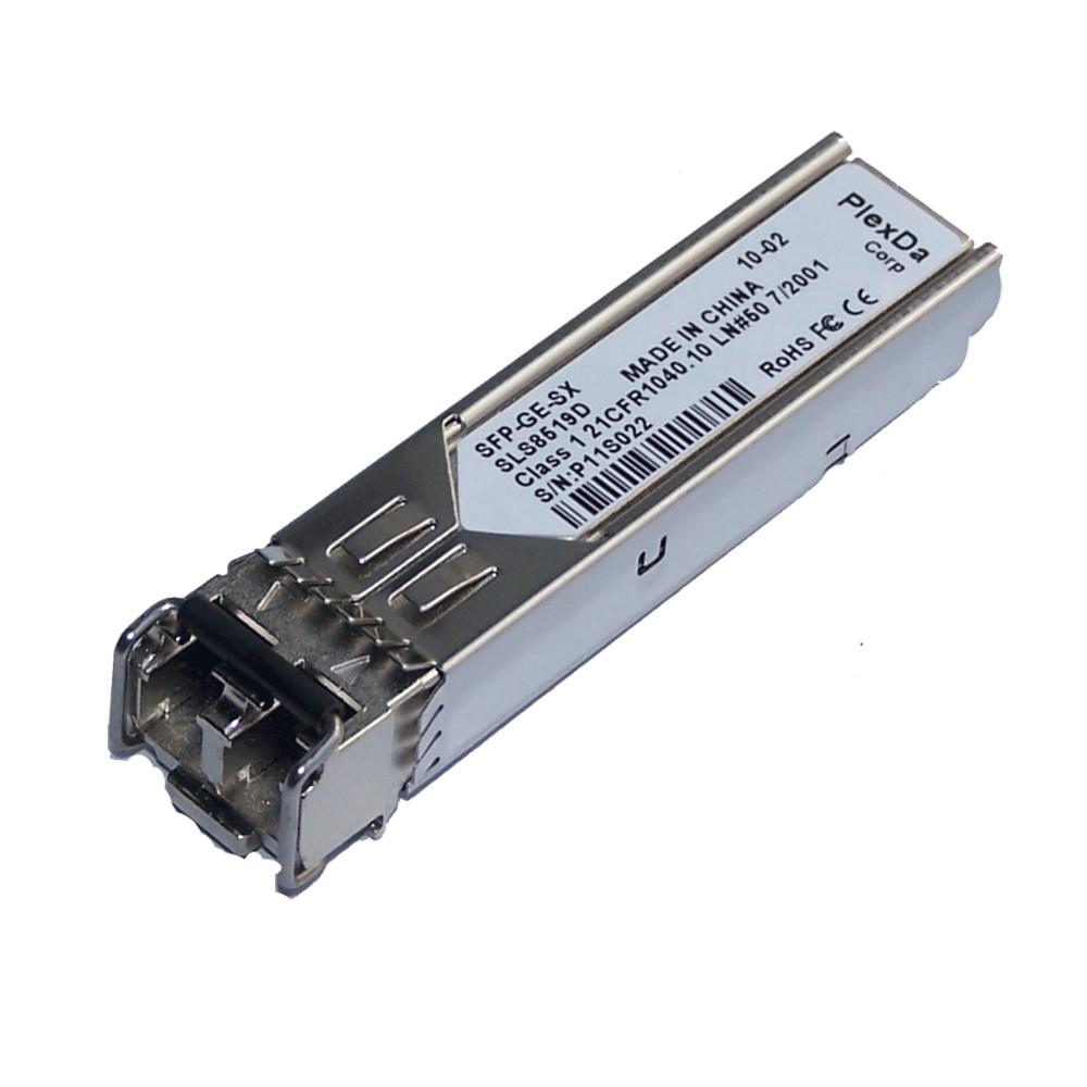
SFP-GE-SX 1.25Gb/s Short-Wavelength SFP Transceive...
SFP-FE-S20 155Mb/s Long-Wavelength SFP Transceiver
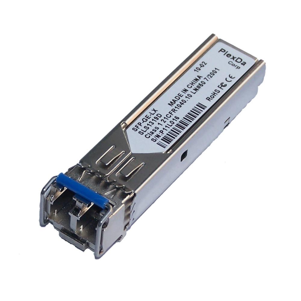
SFP-GE-LX 1.25Gb/s Long-Wavelength SFP Transceiver...
SFP-FE-S40 155Mb/s Long-Wavelength SFP Transceiver
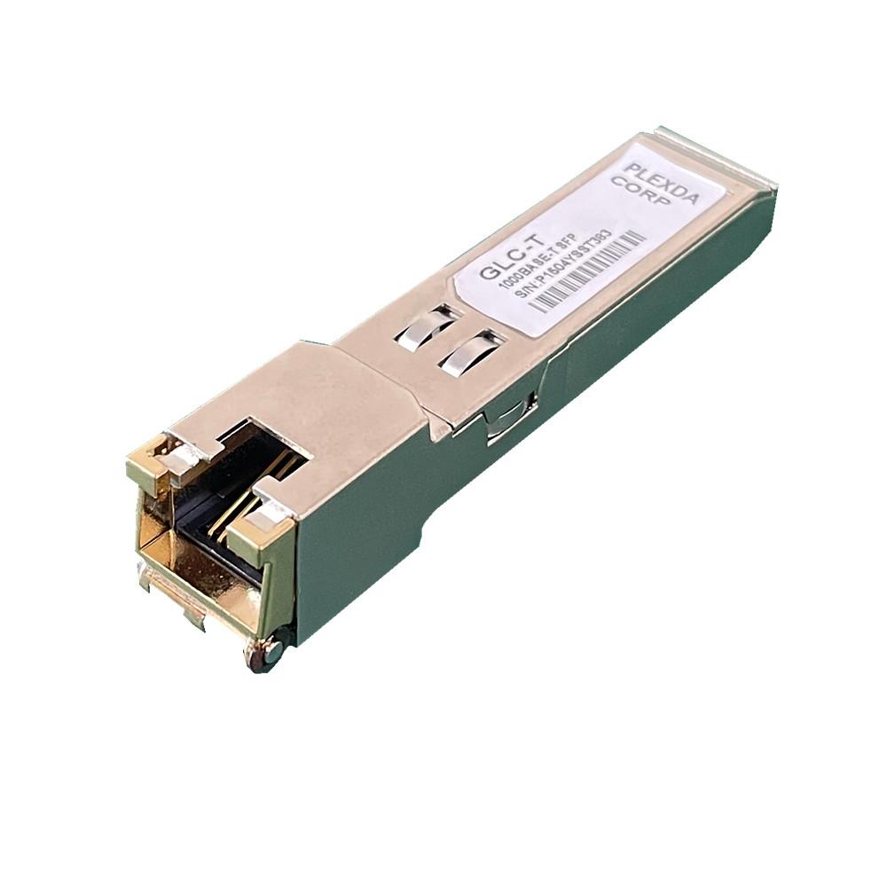
SFP-T 10/100/1000BASE-T Copper SFP Transceiver Dat...
SFP-FE-S80 155Mb/s Long-Wavelength SFP Transceiver

 English
 Chinese