Product
Plexda SFP+, SFP, SFF, QSFP, CFP, Ethernet media converter, POE switch,200G AOC cable OEM factory
Plexda SFP+, SFP, SFF, QSFP, CFP, Ethernet media converter, POE switch,200G AOC cable OEM factory

Tel:0755-28482291
Hotline:13728624948
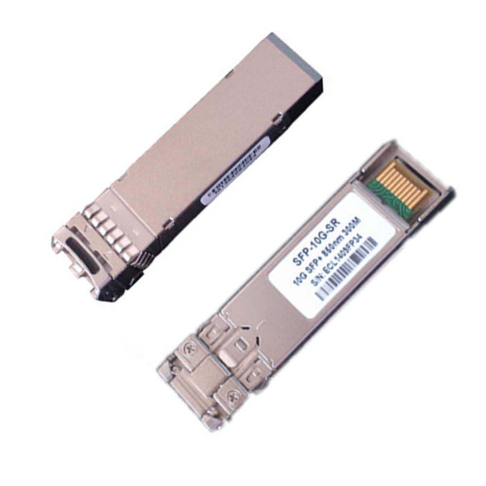
Local:Home > Product > Optical Transceiver > SFP+
Features
◎ Supports 10Gb/s serial optical interface
◎ Up to 10km transmission on SMF
◎ 1310nm DFB laser and PIN receiver
◎ Hot-pluggable SFP+ footprint
◎ SFI high speed electrical interface
◎ Built-in digital diagnostic functions
◎ Single +3.3V power supply
◎ Power consumption less than 1.0 W
◎ Operating case temperature: -5~+70°C
◎ SFP+ MSA package with duplex LC connector
Applications
◎ 10GBASE-LR/LW 10G Ethernet
◎ Other optical links
Standard
◎ Compliant with SFF-8472 and SFP+ MSA
◎ Compliant to SFF-8431 and SFF-8432
◎ Compliant with IEEE 802.3ae 10GBASE-LR/LW
◎ Compliant with FCC 47 CFR Part 15, Class B
◎ Compliant with Telcordia GR-468-CORE
◎ RoHS Compliant
Table 1. Regulatory Compliance
Table 1. Regulatory Compliance
Feature | Standard | Performance |
Electrostatic Discharge(ESD) to the Electrical Pins | MIL-STD-883E Method 3015.7 | Class 1(>1000V for SFI pins, >2000V for other pins.) |
Electrostatic Discharge (ESD) to the Duplex LC Receptacle | IEC 61000-4-2 GR-1089-CORE | Compatible with standards |
Electromagnetic nterference (EMI) | FCC Part 15 Class B EN55022 Class B (CISPR 22B) VCCI Class B | Compatible with standards |
Immunity | IEC 61000-4-3 | Compatible with standards |
Laser Eye Safety | FDA 21CFR 1040.10 and 1040.11 | Compatible with Class I laserproduct |
RoHS | 2002/95/EC 4.1&4.2 2011/65/EU | Compatible with standards |
Product Description
The SFP+ transceivers are high performance, cost effective modules supporting data rate of 10Gbps and 10km transmission distance with SMF.
The transceiver consists of three sections: a Un-cooled 1310nm DFB lasertransmitter, a PIN photodiode integrated with a trans-impedance preamplifier (TIA) and MCU control unit. All modules satisfy class I laser safety requirements.
The transceivers are compatible with SFP Multi-Source Agreement and SFF-8472 digital diagnostics functions.
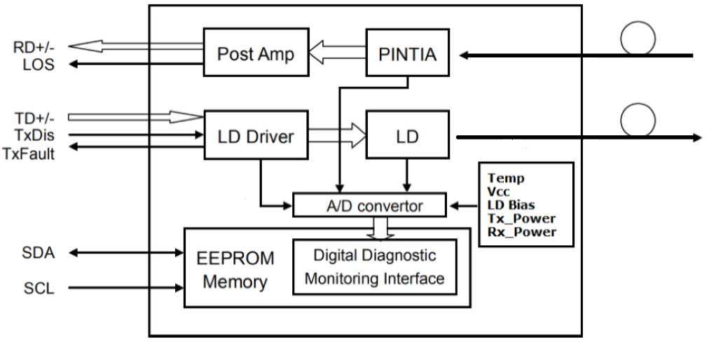
Figure 1.Transceiver functional Block Diagram
Absolute Maximum Ratings
Table 2. Absolute Maximum Ratings
(Exceeding the limits below may damage the transceiver module permanently)
Parameter | Symbol | Min | Typ | Max | Unit | Notes |
Maximum Supply Voltage | VCC | -0.5 | - | +4.0 | V | |
Storage Temperature | TS | -40 | - | +85 | °C | |
Case Operating Temperature | TA | -10 | - | +75 | °C | |
Relative Humidity | RH | 5 | - | 85 | % | 1 |
Notes:
1. Non-condensing.
Recommend Operation Environment
Table 3. Recommend Operation Environment
Parameter | Symbol | Min | Typ | Max | Unit | Notes |
Data Rate | BR | 9.9528 | 10.3125 | 11.3168 | Gbps | |
Power Supply Voltage | VCC | 3.13 | 3.3 | 3.47 | V | |
Power Supply Current | ICC | - | - | 300 | mA | |
Power Dissipation | PD | - | - | 1.0 | W | |
Case Operating Temperature | TA | -5 | - | +70 | °C | |
Transmission Distance | TD | - | - | 10 | km | 1 |
Notes:
1. Measured with ITU-T G.652 SMF
Optical Characteristics
Table 4. Optical Characteristics(TOP = -5 to +70 °C, VCC = 3.13 to 3.47 V)
Parameter | Symbol | Min | Typ | Max | Unit | Notes |
Transmitter | ||||||
Optical Center Wavelength | λC | 1290 | 1310 | 1330 | nm | |
Data Rate | BR | 9.9528 | 10.3125 | 11.3168 | Gbps | |
Average Output Power | PO | -8.2 | - | +0.5 | dBm | 1 |
Optical Modulation Amplitude | POMA | -5.2 | - | - | dBm | 1 |
Optical Extinction Ratio | ER | 3.5 | 5.0 | - | dB | 2 |
RMS Spectral Width (-20dB) | Δλ | - | - | 1 | nm | |
Side Mode Suppression Ratio | SMSR | 30 | - | - | dB | |
Optical Rise/Fall time 20%~80% | Tr/Tf | - | - | 26 | ps | |
Data Dependent Jitter | DDJ | - | - | 0.10 | UI | |
Total Jitte | TJ | - | - | 0.28 | UI | |
Transmitter and Dispersion Penalty | TDP | - | - | 3.2 | dB | |
Average Launch power of Tx OFF | POFF | - | - | -30 | dBm | |
Optical Eye Mask | Compliant with IEEE 802.3ae-2005 and ITU-T G.691 | |||||
Receiver | ||||||
Center Wavelength Range | λC | 1260 | - | 1620 | nm | |
Data Rate | BR | 9.9528 | 10.3125 | 11.3168 | Gbps | |
Receiver Sensitivity | RSEN | - | - | -14.4 | dBm | 3 |
Stressed Receiver Sensitivity (OMA) | RSENS | - | - | -12.6 | dBm | |
Maximum Input Power | PMAX | 0.5 | - | - | dB | 3 |
LOS Assert | LOSA | -28 | - | - | dBm | |
LOS De-Assert | LOSD | - | - | -16 | dBm | |
LOS Hysteresis | LOSH | 0.5 | - | 5 | dB | |
Receiver Reflectance | RR | - | - | -12 | dB | |
Notes:
1. The optical power is launched into SMF.
2. Measured with worst ER=3.5dB, RPBS 2^31-1 test pattern @10.3125Gbs.
3. Measured with worst ER=3.5dB, RPBS 2^31-1 test pattern @10.3125Gbs BER=<10^-12.
Electricalptical Characteristics
Table 5. Electrical Characteristics(TOP = -5 to +70 °C, VCC = 3.13 to 3.47 V)
Parameter | Symbol | Min | Typ | Max | Unit | Notes |
Transmitter | ||||||
Differential Data Input Amplitude | VIN,P-P | 180 | - | 850 | mVpp | 1 |
Input Differential Impedance | ZIN | 80 | 100 | 120 | Ω | |
Transmitter Fault Output-High | VOH | 2.4 | - | VCC | V | |
Transmitter Fault Output-Low | VOL | -0.3 | - | 0.4 | V | |
Transmitter Disable Voltage- High | VIH | 2.0 | - | VCC | V | |
Transmitter Disable Voltage- low | VIL | 0 | - | 0.8 | V | |
Receiver | ||||||
Differential output voltage swing | VOUT,P-P | 300 | - | 850 | mVpp | 1 |
Output Differential Impedance | ZOUT | 80 | 100 | 120 | Ω | |
Data Output Rise/Fall time20%~80% | Tr/Tf | - | - | 28 | ps | 2 |
Deterministic Jitter | DJ | - | - | 0.42 | UI | |
Total Jitte | TJ | - | - | 0.70 | UI | |
LOS Output Voltage-High | VLOSH | 2.0 | - | VCC | V | 3 |
LOS Output Voltage-Low | VLOSL | - | - | 0.8 | V | 3 |
Notes:
1. CML input/output, internally AC-coupled and terminated.
2. Measured with Module Compliance Test Board and OMA test pattern.
3. LOS is an open collector output. Should be pulled up with 4.7kΩ to 10kΩ on the host board.
Normal operation is logic 0; loss of signal is logic 1.
Table 6. Timing and Electrical

Pin Assignment
Table 7. Pin Descriptions

Notes:
1. Open collector/drain output, which should be pulled up with a 4.7kΩ to 10kΩ resistor on the host
board if intended for use. Pull up voltage should be between 2.0V to 3.6V. A high output indicates
a transmitter fault caused by either the TX bias current or the TX output power exceeding the
preset alarm thresholds. A low output indicates normal operation. In the low state, the output is
pulled to <0.8V.
2. Laser output disabled on Tx_Disable >2.0V or open, enabled on Tx_Disable <0.8V.
3. LOS is open collector output. Should be pulled up with 4.7kΩ to 10kΩ on host board to a voltage
between 2.0V and 3.6V. Logic 0 indicates normal operation; logic 1 indicates loss of signal.
4. RD-/+: These are the differential receiver outputs. They are internally AC-coupled 100Ω
differential lines which should be terminated with 100Ω (differential) at the user SERDES.
5. TD-/+: These are the differential transmitter inputs. They are internally AC-coupled, differential
lines with 100Ω differential termination inside the module.

Digital Diagnostic Memory Map
The transceivers provide serial ID memory contents and diagnostic information about the present operating conditions by the 2-wire serial interface (SCL, SDA).
The diagnostic information with internal calibration or external calibration all are implemented, including received power monitoring, transmitted power monitoring, bias current monitoring, supply voltage monitoring and temperature monitoring.
The digital diagnostic memory map specific data field defines as following.
Table 8. Digital Diagnostic Memory Map (Specific Data Field Descriptions)

Table 9. Digital Diagnostic Monitor Characteristics
Parameter | Calibration | Range | Accuracy | Unit |
Transceiver Internal Temperature | Internal | -5 to +70°C | ±3.0 | °C |
VCC3 Internal Supply Voltage | Internal | 3.0 to 3.6V | ±3.0 | % |
Laser Bias Current | Internal | 0 to 90mA | ±10 | % |
Tx Output Power | Internal | -8.5 to +1dBm | ±3.0 | dBm |
Rx Input Power | Internal | -15.5 to +0.5dBm | ±3.0 | dBm |
Recommended Circuit
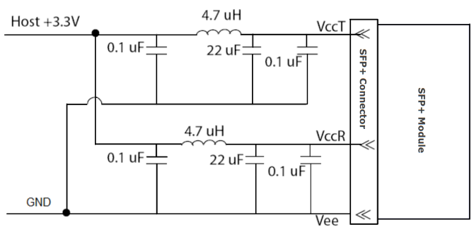
Figure 3, Recommended Host Board Power Supply Circuit
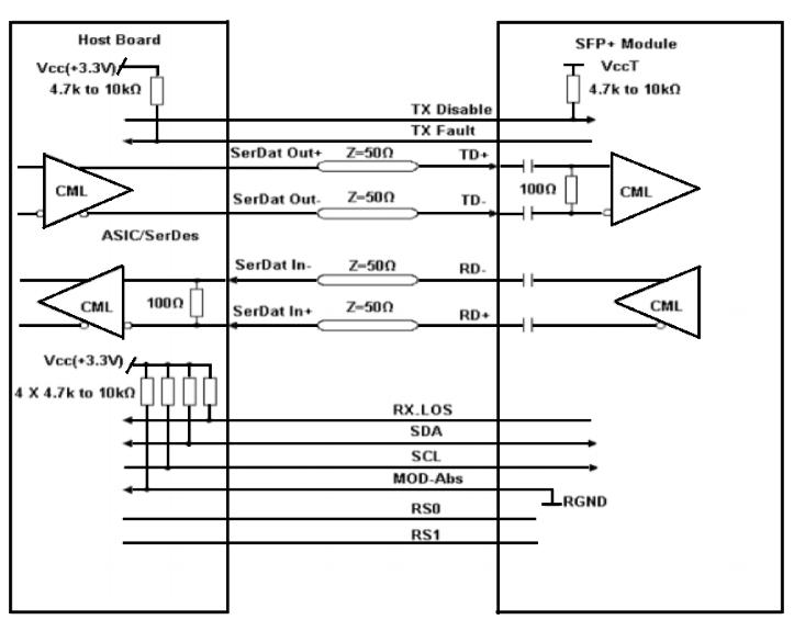
Figure 4, Recommended Interface Circuit
Mechanical Dimensions
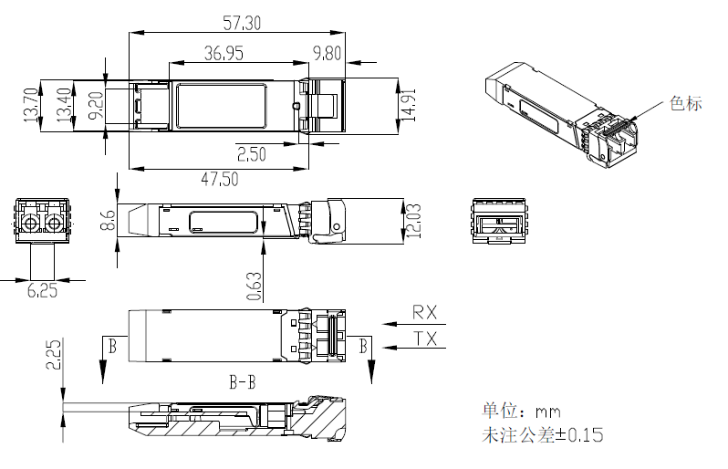
Figure 5, Mechanical Dimensions
Ordering information
Table 10. Ordering information
Part Number | Product Description |
SFP-10G-LR | 1310nm DFB, 10.3125Gbps, SMF 10km, -5°C ~ +70°C |
SFP-10G-LR-E | 1310nm DFB, 10.3125Gbps, SMF 10km, -20°C ~ +85°C |
SFP-10G-LR-I | 1310nm DFB, 10.3125Gbps, SMF 10km, -40°C ~ +85°C |
Warnings
Handling Precautions: This device is susceptible to damage as a result of electrostatic discharge (ESD). A static free environment is highly recommended. Follow guidelines according to proper ESD procedures.
Laser Safety: Radiation emitted by laser devices can be dangerous to human eyes.
Avoid eye exposure to direct or indirect radiation.

 English
 Chinese