Product
Plexda SFP+, SFP, SFF, QSFP, CFP, Ethernet media converter, POE switch,200G AOC cable OEM factory
Plexda SFP+, SFP, SFF, QSFP, CFP, Ethernet media converter, POE switch,200G AOC cable OEM factory

Tel:0755-28482291
Hotline:13728624948
Local:Home > Product > Optical Transceiver > 40G QSFP SR4
Features
◎ Up to 10.3125Gbps Data rate per channel
◎ Up to 100m on OM3 and 150 on OM4 MMF
◎ 4 channels850nm VCSEL array
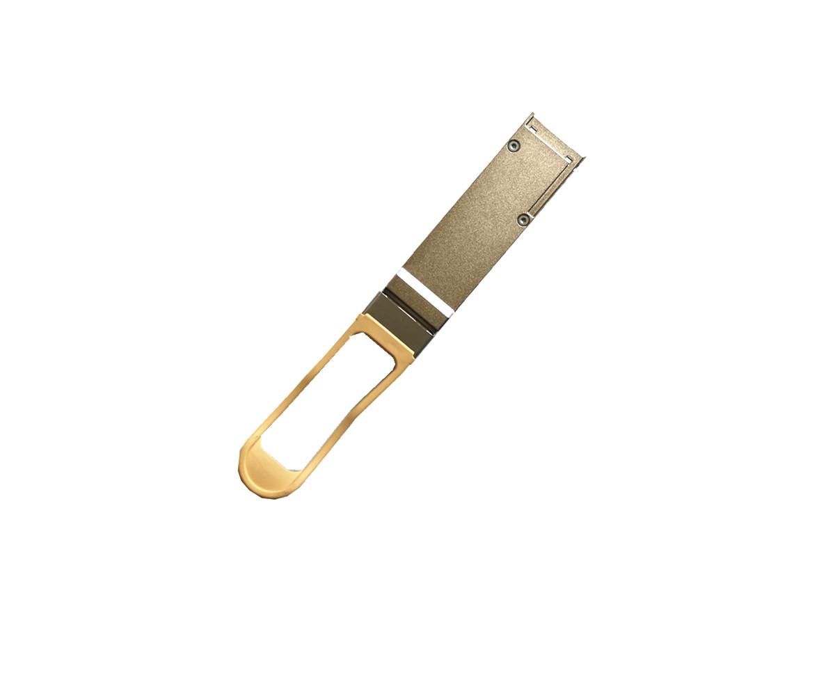
◎ Hot-pluggable QSFP+ form factor
◎ Single MPO connector receptacle
◎ Built-in digital diagnostic functions
◎ Single +3.3V power supply
◎ Low power consumption<1.2 W
◎ Operating case temperature: 0~+70°C
◎ 4 channel full duplex transceiver modules
Applications
◎ 40GBASE-SR4 40G Ethernet
◎ Breakout to 4 x 10GBASE-SR Ethernet
◎ Other optical links
Standard
◎ Compliant with SFF-8436 Specification and QSFP+ MSA
◎ Compliant with IEEE 802.3ba 40GBASE-SR4
◎ Compliant with Telcordia GR-468-CORE
◎ RoHS Compliant
Table 1. Regulatory Compliance
Product Certificate | Certificate Number | Applicable Standard |
TUV | R50135086 | EN 60950-1:2006+A11+A1+A12+A2 EN 60825-1:2014 EN 60825-2:2004+A1+A2 |
UL | E317337 | UL 60950-1 CSA C22.2 No. 60950-1-07 |
EMC CE | AE 50285865 0001 | EN 55022:2010 EN 55024:2010 |
FCC | WTF14F0514417E | 47 CFR PART 15 OCT., 2013 |
FDA | / | CDRH 1040.10 |
ROHS | / | 2011/65/EU |
Product Description
The transceiver is a four-channel, pluggable, parallel, fiber-optic QSFP+ SR4 transceiver module for 40GBASE-SR4 and 40G Ethernet, InfiniBand QDR applications. This high performance module is designed for data communication and interconnect applications. It integrates four data lanes in each direction with 40Gb/s bandwidth. Each lane can operate at 10.3125Gb/s up to 100m transmission distance using OM3 fiber or 150m transmission distance using OM4 fiber. These modules are designed to operate over multimode fiber systems using a nominal wavelength of 850nm. The electrical interface uses a 38 pin contact edge type connector. The optical interface uses an 12 fiber MTP(MPO) connector. This module incorporates Technologies proven circuit and Optical technology to provide reliable long life, high performance and service.

Absolute Maximum Ratings
Table 2. Absolute Maximum Ratings
(Exceeding the limits below may damage the transceiver module permanently)
Parameter | Symbol | Min | Typ | Max | Unit | Notes |
Maximum Supply Voltage | VCC | -0.5 | - | +4.0 | V | |
Storage Temperature | TS | -40 | - | +85 | °C | |
Case Operating Temperature | TA | -5 | - | +75 | °C | |
Relative Humidity | RH | 5 | - | 95 | % | 1 |
Receiver Damage Threshold, each lane | PRdmg | 3.4 | - | - | dBm |
Notes:
1. Non-condensing.
Recommend Operation Environment
Table 3. Recommend Operation Environment
Parameter | Symbol | Min | Typ | Max | Unit | Notes |
Data Rate,each lane | BR | - | 10.3125 | - | Gbps | |
Power Supply Voltage | VCC | 3.13 | 3.3 | 3.47 | V | |
Power Supply Current | ICC | - | - | 360 | mA | |
Power Dissipation | PD | - | - | 1.2 | W | |
Case Operating Temperature | TA | 0 | - | +70 | °C | |
Relative Humidity | RH | 5 | - | 85 | % | 1 |
Transmission Distance | TD | - | - | 100 | m | OM3 *2 |
Transmission Distance | TD | - | - | 150 | m | OM4 *2 |
Notes:
1. Non-condensing.
2. Measured with ITU-T G.651 OM3 MMF and OM4 MMF
Electricalptical Characteristics
Table 4. Electrical Characteristics(TOP = 0 to +70 °C, VCC = 3.13 to 3.47 V)
Parameter | Symbol | Min | Typ | Max | Unit | Notes |
Transmitter | ||||||
Differential Data Input Amplitude | VIN,P-P | 180 | - | 900 | mVpp | |
Input Differential Impedance | ZIN | 90 | 100 | 110 | Ω | |
Transmitter Fault Output-High | VOH | 2.4 | - | VCC | V | |
Transmitter Fault Output-Low | VOL | -0.3 | - | 0.4 | V | |
Transmitter Disable Voltage- High | VIH | 2.0 | - | VCC | V | |
Transmitter Disable Voltage- low | VIL | 0 | - | 0.8 | V | |
Receiver | ||||||
Differential output voltage swing | VOUT,P-P | 300 | - | 900 | mVpp | |
Output Differential Impedance | ZOUT | 90 | 100 | 110 | Ω | |
LOS Output Voltage-High | VLOSH | 2.0 | - | VCC | V | |
LOS Output Voltage-Low | VLOSL | - | - | 0.8 | V | |
Optical Characteristics
Table 5. Optical Characteristics(TOP = 0 to +70 °C, VCC = 3.13 to 3.47 V)
Parameter | Symbol | Min | Typ | Max | Unit | Notes |
Transmitter | ||||||
Optical Center Wavelength | λC | 840 | 850 | 860 | nm | |
RMS Spectral Width | σ | - | - | 0.6 | nm | |
Data Rate, each lane | BR | - | 10.3125 | - | Gbps | |
Average Launch Power,each lane | PO | -7.6 | - | -1 | dBm | 1 |
Optical Modulation Amplitude, each lane | POMA | -5.6 | - | 3.0 | dBm | |
Optical Extinction Ratio | ER | 3.0 | - | - | dB | |
Transmitter and dispersion eye closure, each lane | TDEC | - | - | 3.5 | dBm | |
Launch Power(OMA) minus TDEC, each lane | P-TDEC | -6.5 | - | - | dBm | |
Optical Return Loss Tolerance | ORL | - | - | 12 | dB | |
Average Launch power of Tx OFF, each lane | POFF | - | - | -30 | dBm | |
Transmitter Eye Mask coordinates: X1, X2, X3, Y1, Y2, Y3 | SPECIFICATION VALUES {0.23, 0.34, 0.43, 0.27, 0.35, 0.4 } | 2 | ||||
Receiver | ||||||
Center Wavelength Range | λC | 840 | 850 | 860 | nm | |
Data Rate, each lane | BR | - | 10.3125 | - | Gbps | |
Receiver Power(OMA), each lane | POMA | - | - | 3.0 | dBm | |
Average Receive Power, each lane | RPO | -9.9 | - | +2.4 | dBm | 1 |
Receiver Sensitivity(OMA), each lane | RSEN | - | - | -9.9 | dBm | 3 |
Stressed Receiver Sensitivity (OMA) , each lane | RSRS | - | - | -5.4 | dBm | |
LOS Assert | LOSA | -28 | - | - | dBm | |
LOS De-Assert | LOSD | - | - | -12 | dBm | |
LOS Hysteresis | LOSH | 0.5 | - | 5.0 | dB | |
Receiver Reflectance | RR | - | - | -12 | dB | |
Notes:
1. Average launch/receive power, each lane (min) is informative and not the principal indicator of signal strength. A transmitter with launch/receive power below this value cannot be compliant; however, a value above this does not ensure compliance.
2. Hit Ratio 10^-12. hits/sample
3. Measured with worst ER=3.0dB, RPBS 2^31-1 test pattern @10.3125Gbps BER=<10^-12.
Pin Assignment
Table 6. Pin Descriptions
Pin | Symbol | Name/Description | Notes |
1 | GND | Ground | 1 |
2 | Tx2n | Transmitter Inverted Data Input | |
3 | Tx2p | Transmitter Non-Inverted Data Input | |
4 | GND | Ground | 1 |
5 | Tx4n | Transmitter Inverted Data Input | |
6 | Tx4p | Transmitter Non-Inverted Data Input | |
7 | GND | Ground | 1 |
8 | ModSelL | Module Select | 2 |
9 | ResetL | Module Reset | 2 |
10 | Vcc Rx | +3.3 V Power supply receiver | |
11 | SCL | 2-wire serial interface clock | 2 |
12 | SDA | 2-wire serial interface data | 2 |
13 | GND | Ground | 1 |
14 | Rx3p | Receiver Non-Inverted Data Output | |
15 | Rx3n | Receiver Inverted Data Output | |
16 | GND | Ground | 1 |
17 | Rx1p | Receiver Non-Inverted Data Output | |
18 | Rx1n | Receiver Inverted Data Output | |
19 | GND | Ground | 1 |
20 | GND | Ground | |
21 | Rx2n | Receiver Inverted Data Output | |
22 | Rx2p | Receiver Non-Inverted Data Output | |
23 | GND | Ground | 1 |
24 | Rx4n | Receiver Inverted Data Output | |
25 | Rx4p | Receiver Non-Inverted Data Output | |
26 | GND | Ground | 1 |
27 | ModPrsL | Module Present | |
28 | IntL | Interrupt | 2 |
29 | Vcc Tx | +3.3 V Power supply transmitter | |
30 | Vcc1 | +3.3 V Power Supply | |
31 | LPMode | Low Power Mode | 2 |
32 | GND | Ground | 1 |
33 | Tx3p | Transmitter Non-Inverted Data Input | |
34 | Tx3n | Transmitter Inverted Data Input | |
35 | GND | Ground | 1 |
36 | Tx1p | Transmitter Non-Inverted Data Input | |
37 | Tx1n | Transmitter Inverted Data Input | |
38 | GND | Ground | 1 |
Notes:
1. Circuit ground is internally isolated from chassis ground.
2. Open collector; should be pulled up with a 4.7kΩ to 10kΩ resistor on host board to a voltage between 3.15Vand 3.6V.
Pin Assignment (continued)

Optical Interface Lanes and Assignment
The optical interface port is a male MPO connector, the keying feature of the MPO receptacle is on the top, then fibers are numbered left to right as 12 through 1 looking into the receptacle. The four fiber positions on the left (fibers 12, 11, 10, 9) are used for the optical transmit signals (Channel 1 through 4). The fiber positions on the right (fibers 4, 3, 2, 1) are used for the optical receive signals (Channel 4 through 1). The central four fibers (5, 6, 7, 8) may be physically present.

Digital Diagnostic Monitoring Interface
Digital diagnostics monitoring function is available on all QSFP+ module. A 2-wire serial interface provides user to contact with module. The structure of the memory is shown in Figure 4. The memory space is arranged into a lower, single page, address space of 128 bytes and multiple upper address space pages. This structure permits timely access to addresses in the lower page, such as Interrupt Flags and Monitors. Less time critical time entries, such as serial ID information and threshold settings, are available with the Page Select function. The interface address used is A0xh and is mainly used for time critical data like interrupt handling in order to enable a one-time-read for all data related to an interrupt situation. After an interrupt, IntL, has been asserted, the host can read out the flag field to determinethe affected channel and type of flag.

Table 7. Digital Diagnostic Monitor Characteristics
Parameter | Calibration | Range | Accuracy | Unit |
Transceiver Internal Temperature | Internal | 0 to +70°C | ±3.0 | °C |
VCC Internal Supply Voltage | Internal | 3.0 to 3.6V | ±3.0 | % |
Laser Bias Current, each lane | Internal | 0 to 20mA | ±10 | % |
Tx Output Power, each lane | Internal | -8.6 to 0dBm | ±3.0 | dBm |
Rx Input Power, each lane | Internal | -14.0 to 0dBm | ±3.0 | dBm |
Table 8. Timing and Electrical
Parameter | Symbol | Min | Typ | Max | Unit |
Initialization Time | t_init | - | - | 2000 | ms |
Reset Init Assert Time | t_reset_init | - | - | 2 | us |
Serial Bus Hardware Ready Time | t_serial | - | - | 2000 | ms |
Monitor Data Ready Time | t_data | - | - | 2000 | ms |
Reset Assert Time | t_reset | - | - | 2000 | ms |
LPMode Assert Time | ton_LPMode | - | - | 100 | us |
IntL Assert Time | ton_IntL | - | - | 200 | ms |
IntL Deassert Time | toff_IntL | - | - | 500 | us |
Rx LOS Assert Time | ton_los | - | - | 100 | ms |
Tx Fault Assert Time | ton_Txfault | - | - | 200 | ms |
Flag Assert Time | ton_flag | - | - | 200 | ms |
Mask Assert Time | ton_mask | - | - | 100 | ms |
Mask Deassert Time | toff_mask | - | - | 100 | ms |
ModSelL Assert Time | ton_ModSelL | - | - | 100 | us |
ModSelL Deassert Time | toff_ModSelL | - | - | 100 | us |
Power_over-ride or Power-set Assert Time | ton_Pdown | - | - | 100 | ms |
Power_over-ride or Power-set Deassert Time | toff_Pdown | - | - | 300 | ms |
Recommended Circuit

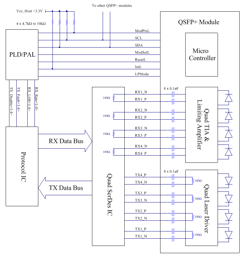
Figure 6, Recommended Interface Circuit
Mechanical Dimensions
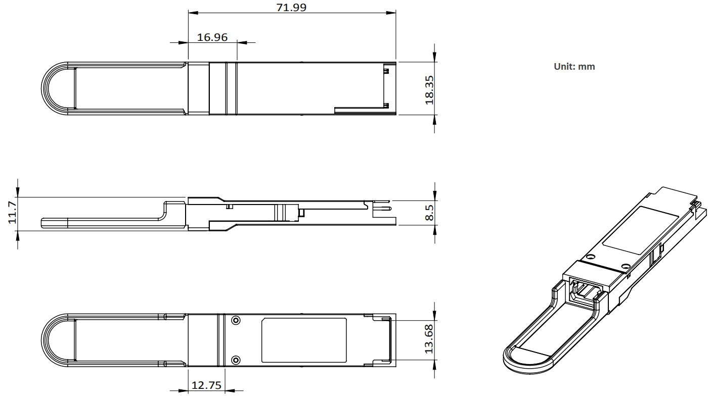
Figure 7, Mechanical Dimensions
Ordering information
Table 9. Ordering information
Part Number | Product Description |
QSFP-40G-SR4 | 850nm array VCSEL, MPO, 41.25Gbps, OM4 MMF 150m, 0°C ~ +70°C |
QSFP-40G-SR4E | 850nm array VCSEL, MPO, 41.25Gbps, OM4 MMF 150m, -20°C ~ +85°C |
QSFP-40G-SR4I | 850nm array VCSEL, MPO, 41.25Gbps, OM4 MMF 150m, -40°C ~ +85°C |
Warnings
Handling Precautions: This device is susceptible to damage as a result of electrostatic discharge (ESD). A static free environment is highly recommended. Follow guidelines according to proper ESD procedures.
Laser Safety: Radiation emitted by laser devices can be dangerous to human eyes.Avoid eye exposure to direct or indirect radiation.

 English
 Chinese