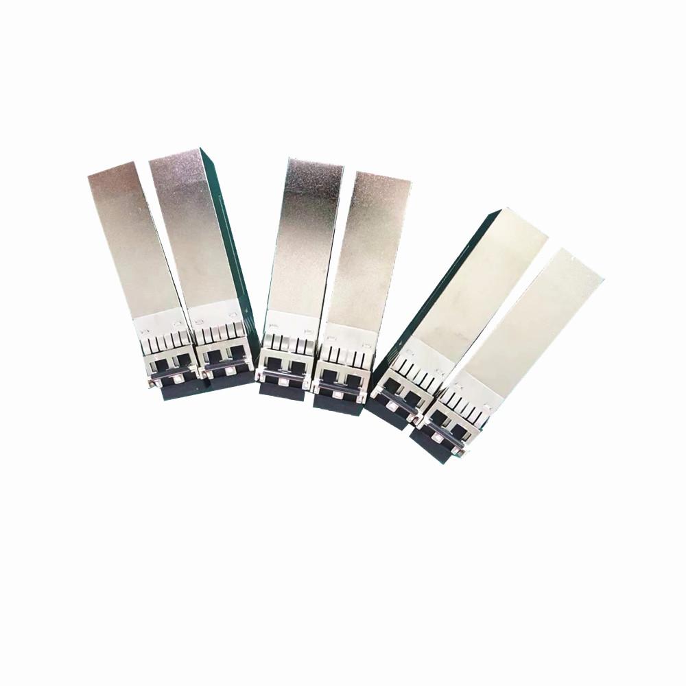
Product
Plexda SFP+, SFP, SFF, QSFP, CFP, Ethernet media converter, POE switch,200G AOC cable OEM factory
Plexda SFP+, SFP, SFF, QSFP, CFP, Ethernet media converter, POE switch,200G AOC cable OEM factory

Tel:0755-28482291
Hotline:13728624948
Local:Home > Product > Optical Transceiver > 25G SFP28 LR
Features
◎ Supports 25.78125Gb/s serial optical interface
◎ Up to 10km transmission on SMF
◎1310nm DFB laser and PIN receiver
◎ Hot-pluggable SFP28 footprint
◎ Built-in digital diagnostic functions
◎ Single +3.3V power supply
◎ Power consumption less than 1.2 W
◎ Operating case temperature: -5~+70°C
◎ Internal CDR on both transmitter and receiver channel
◎Support CDR bypass
◎ SFP28 MSA package with Duplex LC connector
Applications
◎25GBASE-LR25G Ethernet
◎ 25.78125 Gb/s single lane 100GE LR4
◎ Other optical links
Standard
◎ Compliant with SFF-8402 and SFF-8472
◎ Compliant to SFF-8431 and SFF-8432
◎ Compliant with IEEE 802.3by 25GBASE-LR
◎ Compliant with FCC 47 CFR Part 15, Class B
◎ Compliant with Telcordia GR-468-CORE
◎ RoHS Compliant
Table 1. Regulatory Compliance
Product Certificate | Certificate Number | Applicable Standard |
TUV | R50135086 | EN 60950-1:2006+A11+A1+A12+A2 EN 60825-1:2014 EN 60825-2:2004+A1+A2 |
UL | E317337 | UL 60950-1 CSA C22.2 No. 60950-1-07 |
EMC CE | AE 50285865 0001 | EN 55022:2010 EN 55024:2010 |
FCC | WTF14F0514417E | 47 CFR PART 15 OCT., 2013 |
FDA | / | CDRH 1040.10 |
ROHS | / | 2011/65/EU |
Product Description
The SFP28 transceivers are high performance, cost effective modules supporting data rate of 25.78125Gbps and Up to 10km transmission on SMF.
The transceiver consists of three sections: a 1310nm DFB lasertransmitter, a PIN photodiode integrated with a trans-impedance preamplifier (TIA) and MCU control unit. All modules satisfy class I laser safety requirements.
The transceivers are compatible with SFP Multi-Source Agreement and SFF-8472 digital diagnostics functions.
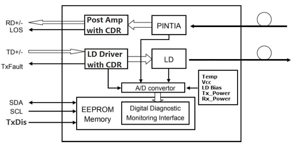
Figure 1.Transceiver functional Block Diagram
Absolute Maximum Ratings
Table 2. Absolute Maximum Ratings
(Exceeding the limits below may damage the transceiver module permanently)

Notes:
1. Non-condensing.
Recommend Operation Environment
Table 3. Recommend Operation Environment

Notes:
1. Measured with ITU-T G.652 SMF
Electricalptical Characteristics
Table 4. Electrical Characteristics(TOP = -5 to +70 °C, VCC = 3.13 to 3.47 V)

Notes:
1. CML input/output, internally AC-coupled and terminated.
Optical Characteristics
Table 5. Optical Characteristics(TOP = -5 to +70 °C, VCC = 3.13 to 3.47 V)

Notes:
1. Measured with worst ER=2.0dB, RPBS 2^31-1 test pattern @25.78125Gbs BER=<5E-5.
Table 6. Timing and Electrical

Pin Assignment
Table 7. Pin Descriptions

Notes:
1. Open collector/drain output, which should be pulled up with a 4.7kΩ to 10kΩ resistor on the host
board if intended for use. Pull up voltage should be between 2.0V to 3.6V. A high output indicates
a transmitter fault caused by either the TX bias current or the TX output power exceeding the
preset alarm thresholds. A low output indicates normal operation. In the low state, the output is
pulled to <0.8V.
2. Laser output disabled on Tx_Disable >2.0V or open, enabled on Tx_Disable <0.8V.
3. LOS is open collector output. Should be pulled up with 4.7kΩ to 10kΩ on host board to a voltage
between 2.0V and 3.6V. Logic 0 indicates normal operation; logic 1 indicates loss of signal.
4. RD-/+: These are the differential receiver outputs. They are internally AC-coupled 100Ω
differential lines which should be terminated with 100Ω (differential) at the user SERDES.
5. TD-/+: These are the differential transmitter inputs. They are internally AC-coupled, differential
lines with 100Ω differential termination inside the module.

Digital Diagnostic Memory Map
The transceivers provide serial ID memory contents and diagnostic information about the present operating conditions by the 2-wire serial interface (SCL, SDA).
The diagnostic information with internal calibration or external calibration all are implemented, including received power monitoring, transmitted power monitoring, bias current monitoring, supply voltage monitoring and temperature monitoring.
The digital diagnostic memory map specific data field defines as following.
Table 8. Digital Diagnostic Memory Map (Specific Data Field Descriptions)

Table 9. Digital Diagnostic Monitor Characteristics

Recommended Circuit
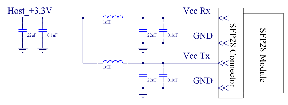
Figure 3, Recommended Host Board Power Supply Circuit
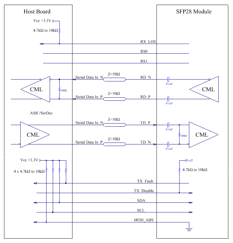
Figure 4, Recommended Interface Circuit
Mechanical Dimensions
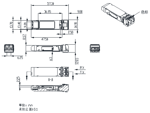
Figure 5, Mechanical Dimensions
Ordering information
Table 10. Ordering information

Warnings
Handling Precautions: This device is susceptible to damage as a result of electrostatic discharge (ESD). A static free environment is highly recommended. Follow guidelines according to proper ESD procedures.
Laser Safety: Radiation emitted by laser devices can be dangerous to human eyes.
Avoid eye exposure to direct or indirect radiation.

 English
 Chinese